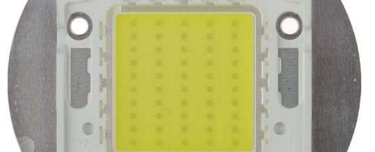
LED package has experienced several technical upgrades, from the first generation of PPA to ceramic substrate, and now comes to the third generation of EMC package. The emerging of new technologies brings unlimited business opportunities to contenders, while also hits the market structure in their field.
EMC (Epoxy Molding Compound) is one of the main raw materials during producing IC (Integrated Circuit). With the development of IC packaging technology, EMC as the main electronic packaging materials has also been developed rapidly. Because of high reliability, low cost, simple production process, suitable for mass production, EMC occupies more than 97 % of the market share in the entire microelectronics packaging materials market. Now, EMC is extending to semiconductor devices, integrated circuits, consumer electronics, automotive, military, aviation and so on. Because of excellent heat resistance and suitable for large-scale production, EMC provides an excellent solution for LED packaging applications.
EMC package is a highly integrated framework that adopts modified epoxy materials and etching technique, the etched copper substrate makes epoxy with greater contact area with copper holder. Respect to thermoplastic PPA, EMC has stronger adhesive force, makes the EMC products have unique advantages on against moisture and Red ink penetration, this package originates from the IC package, but different from it. Due to the changes in materials and structures, EMC products with features of high heat resistance, anti-UV, highly integrated, withstand high current, small size and so on. Especially improved UV resistance significantly, making the EMC product applications expanded greatly, it can be applied to harsh environments as outdoor lamp and automotive lighting, will have great impact to the high-end ceramic packages.
In order to pursuit cost-effective, the use of ultra-current in the LED industry has become a consensus, but there are also high risks on the heat treatment. EMC is outstanding because of its high heat resistance. Currently, the generic packaging technology that EMC used is: adopts normal DA / vertical structure low or middle power chip, low thermal insulation gum as chip adhesive, and then soldering, powder and cutting, finally achieve the finished product.
EMC package will not only change packaging manufacturers, but also influence related companies, such as bracket and equipment factories, especially will bring great impact to the traditional PPA and ceramic bracket market.
ShareJUL
2016
